Low Energy Electron Diffraction Time-Lapse Experiment | |||||||||||||||||||||||||||||||||||||||||||||||||||||||||||||||||||||||||||||||||||||
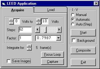
This following time-lapse experiment demonstrates voltage changes and diffraction pattern responses using a LEEDS system developed by OCI Vacuum Microengineering in LONDON, Ontario and Northern Eclipse. Primary beam energy variation was in the range of 40eV to 150eV. The 1x1 pattern identifies the Si(111) sample after a short thermal treatment (up to 1000 degrees C) at a vacuum of 10 -9 Torr. Data and images were taken using an INTEGRALEED spectrometer, model BDL800IR with NORTHERN ECLIPSE imaging analysis system and a PRINCETON MICROMAX cooled digital CCD camera. For information on the INTEGRALEED spectrometer contract OCI at 519-457-0878 or Email oci@gtn.net |
|||||||||||||||||||||||||||||||||||||||||||||||||||||||||||||||||||||||||||||||||||||
![]() |
![]() |
![]() |
|||||||||||||||||||||||||||||||||||||||||||||||||||||||||||||||||||||||||||||||||||
![]() |
|||||||||||||||||||||||||||||||||||||||||||||||||||||||||||||||||||||||||||||||||||||
![]() |
|
![]() |
|||||||||||||||||||||||||||||||||||||||||||||||||||||||||||||||||||||||||||||||||||
|